


 |
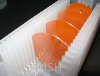
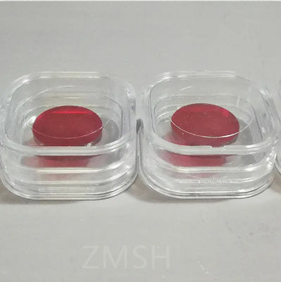
GaP Wafer Gallium Phosphide Single Crystal Orientation (111)A 0°±0.2 Solar Cells
Product Details:
| Place of Origin: | China |
| Brand Name: | ZMSH |
| Model Number: | GaP wafer |
|
Detail Information |
|||
| Thickness: | Min:175 Max:225 | Dopant: | S |
|---|---|---|---|
| Surface Finish-back: | Polished | Particle Count: | N/A |
| Edge Rounding: | 0.250mmR | IF Location/Length: | EJ[0-1-1]/ 7±1mm |
| Conduct Type: | S-C-N | Epi-Ready: | Yes |
| Highlight: | GaP Wafer Semiconductor Substrate,Gallium Phosphide Single Crystal Orientation,Gallium Phosphide GaP Wafer |
||
Product Description
GaP Wafer, Gallium Phosphide single crystal Orientation (111)A 0°±0.2 Solar Cells
Product Description:
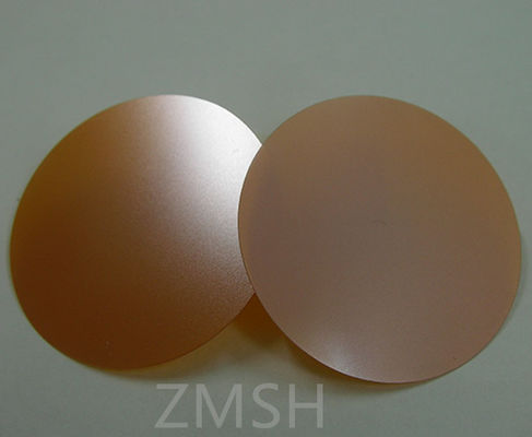
Gallium Phosphide GaP, an important semiconductor of unique electrical properties as other III-V compound materials, crystallizes in the thermodynamically stable cubic ZB structure, is an orange-yellow semitransparent crystal material with an indirect band gap of 2.26 eV (300K), which is synthesized from 6N 7N high purity gallium and phosphorus, and grown into single crystal by Liquid Encapsulated Czochralski (LEC) technique. Gallium Phosphide crystal is doped sulfur or tellurium to obtain n-type semiconductor, and zinc doped as p-type conductivity for further fabricating into desired wafer, which has applications in optical system, electronic and other optoelectronics devices. Single Crystal GaP wafer can be prepared Epi-Ready for your LPE, MOCVD and MBE epitaxial application. High quality single crystal Gallium phosphide GaP wafer p-type, n-type or undoped conductivity at Western Minmetals (SC) Corporation can be offered in size of 2″and 3” (50mm, 75mm diameter) , orientation <100>,<111> with surface finish of as-cut, polished or epi-ready process.
Features:
- Wide bandgap suitable for emitting specific wavelengths of light.
- GaP Wafer Excellent optical properties enabling LED production in various colors.
- High efficiency in generating red, yellow, and green lights for LEDs.
- Superior light absorption ability at specific wavelengths.
- Good electrical conductivity facilitating high-frequency electronic devices.
- GaP Wafer Appropriate thermal stability for reliable performance.
- Chemical stability suitable for semiconductor manufacturing processes.
- GaP Wafer Favorable lattice parameters for epitaxial growth of additional layers.
- Capability to serve as a substrate for semiconductor deposition.
- GaP Wafer Robust material with high thermal conductivity.
- Excellent optoelectronic capabilities for photodetectors.
- Versatility in designing optical devices for specific wavelength ranges.
- GaP Wafer Potential application in solar cells for tailored light absorption.
- Relatively matched lattice structures for quality semiconductor growth.
- Essential role in LED, laser diode, and photodetector fabrication due to its optical and electrical properties.
Technical Parameters:
| Parameter | Value |
|---|---|
| Growth Method | LEC |
| BOW | Max:10 |
| Diameter | 50.6±0.3mm |
| Particle Count | N/A |
| Orientation Angle | N/A |
| TTV/TIR | Max:10 |
| Dopant | S |
| Laser Marking | N/A |
| Orientation | (111)A 0°±0.2 |
| Mobility | Min:100 |
| Semiconductor Material | Semiconductor Substrate |
| Surface Oxidation | Ultra-thick Silicon Oxide Wafer |
Applications:
- GaP Wafer LED manufacturing for producing red, yellow, and green lights.
- GaP Wafer Laser diode fabrication for diverse optical applications.
- GaP Wafer Photodetector development for specific wavelength ranges.
- GaP Wafer Utilization in optoelectronic sensors and light sensors.
- GaP Wafer Solar cell integration for tailored light spectrum absorption.
- GaP Wafer Production of display panels and indicator lights.
- GaP Wafer Contribution to high-frequency electronic devices.
- GaP Wafer Formation of optical devices for distinct wavelength ranges.
- GaP Wafer Usage in telecommunications and optical communication systems.
- GaP Wafer Development of photonic devices for signal processing.
- GaP Wafer Incorporation in infrared (IR) and ultraviolet (UV) sensors.
- GaP Wafer Implementation in biomedical and environmental sensing devices.
- GaP Wafer Application in military and aerospace optical systems.
- GaP Wafer Integration into spectroscopy and analytical instrumentation.
- GaP Wafer Utilization in research and development for emerging technologies.
Customization:
Brand Name: ZMSH
Model Number: GaP wafer
Place of Origin: China
TTV/TIR: Max:10
BOW: Max:10
OF Location/Length: EJ[0-1-1]/ 16±1mm
Mobility: Min:100
Resistivity: Min:0.01 Max:0.5 Ω.cm
Features:
• Using thin film technology
• Silicon oxide wafer
• Electro-oxidation
• Customized service
Support and Services:
We provide a wide range of technical support and services for our Semiconductor Substrate products. Our team of experts are available to provide you with the best solutions for your needs.
Whether you need advice on product selection, installation, testing, or any other technical issue, we are here to help. We offer a variety of services, including:
- Product selection and evaluation
- Installation and testing
- Troubleshooting and problem solving
- Performance optimization
- Product training and education
Our team of experienced engineers and technicians are available to answer any of your questions and provide the best technical advice and support. Contact us today and let us help you find the best solution for your needs.